2012年2月12日星期日

1.5v LED FLASHER


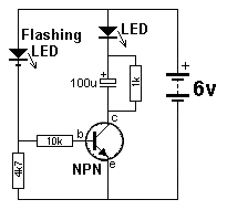
The next circuit flashes a LED and uses a 1.5v supply. The LED does not turn on via the 1k resistor because the characteristic voltage of a LED is between 1.7v and 2.3v, (depending on the colour).  It turns on when the 100u is "jacked up" by the collector of the BC557.
The circuit is a charge-pump design. This is where a capacitor (electrolytic) is allowed to charge and is then raised higher and allowed to discharge into a load. The load sees a voltage that can be higher than the supply.
The two transistors operate as a high-gain amplifier with the output being the 47R. The cycle starts with the first transistor being turned on via the 100k. This action also charges the 10u until 0.75v appears on the base of the transistor.
This turns on the second transistor and the negative end of the 10u is raised when the BC557 turns on. This raises the positive end of the 10u and the first transistor turns on even more. This action continues until the first transistor is fully turned on and the BC557 is fully turned on. The voltage across the collector-emitter terminals of the BC557 will be small and about 1v will appear across the 47R. This voltage "jacks up" the 100u and since it is fully charged via the 1k resistor, it will present a voltage of about 2.5v to the LED. Any voltage over 1.7v will turn on a red LED and a green LED will turn on at 2.3v. The energy in the 100u is now passed to the LED to illuminate it.
The flash is very brief due to the operation of the two-transistor amplifier. Although the energy in the 100u will produce a brief flash, the timing of the two transistor circuit is even faster and it provides the duration. The actual duration of the flash depends on the time the two transistor amplifier can be in a fully turned-on state. This is governed by the charging of the 10u electrolytic.
When the base of the first transistor sees 0.7v, the two transistors start to turn on by a process called REGENERATION. This is explained further in our article: REGENERATION, in Circuit Tricks. Regeneration is a condition where a circuit turns on more and more without any external assistance.

The 10u is "jacked up" by the BC557 turning on and it delivers a current to the base of the BC547. Initially it delivers its energy to the base but very soon is is higher than 0.7v and it is fully discharged. The electrolytic now starts to charge in the reverse direction and this process continues to keep the BC 547 turned on. It charges very quickly in the reverse direction as the charging path is the emitter-collector junction of the BC557 and base-emitter junction of the BC547. When it is nearly charged, the current-flow reduces and this turns off the BC547 very slightly. This turns off the BC557 slightly and the 10u is "lowered." This puts less "turn-on" on the BC547 and the two transistors start to turn off very quickly.
The 10u is now charged in the reverse direction and a negative voltage is presented to the base of the first transistor. This voltage is is gradually reduced by the electrolytic charging via the 100k and that's why the circuit has a very long off cycle.Two circuits are shown. They use slightly different components to produce the same results.
The only critical value is the 100R. The circuit will not work with a value higher than about 150R. It needs a low value so the BC557 transistor is turned on to a high level before a voltage is developed across the 100R. If the value is too high, a voltage will be developed across this resistor when the BC557 is turned on a small amount and this voltage will be sent to the BC547 to turn it on too. The two transistor will sit in a conditions that they are both turned on and the circuit will freeze.
The circuit has to function such that the BC547 is turned on to its maximum when the electrolytic is pulled HIGH. This transistor will now be turned on by the current delivered by the 100k (or 1M) plus the charging current of the electrolytic.  As the electrolytic charges, the current into the base of the BC547 will fall and the transistor will turn off slightly. This slight turn-off must be passed to the BC557 to turn it off slightly too and lower the "turn-on" effect of the electrolytic. It is the 47R (or 100R) that is pulling the electrolytic down to the 0v rail and if this resistor does not have sufficient "pull-down" effect, the cycle will not continue. When this resistor has a low value, the BC557 must deliver a high current and it must be turned on via a proportionally high current into the base. This current comes from the BC547 and it needs a proportionally high current into its base to provide this condition. We are only talking about fractions of milliamps and microamps, but these conditions must be met for the circuit to work.   www.bgocled.com 

THE FLIP FLOP LED


Here are some Flashing LED circuits from "200 Transistor Circuits' eBook. The first 4 circuits show how to change an NPN transistor for PNP.


2011年12月28日星期三

Who needs a 92-inch TV? Mitsubishi, the guys who make it


The mammoth 92-inch TV Mitsubishi will start selling next month.
(Credit:
Mitsubishi)

Does a 92-inch TV sound like overkill to you?
To many, it may. But for the company that makes it, Mitsubishi, it’s pretty much the only way to distinguish itself among its competitors and try to stay in the TV business.
Next month, Mitsubishi will officially start selling the behemoth of a television it first introduced at CES in January. The 92-inch 840 3D DLP Home Cinema TV will cost $5,999, has a resolution of 1080p, uses DLP rear-projection technology, and can display 3D content. It also comes in 72 inches and 83 inches.
Yes, there will be people that will buy it. The kind of people who, say, have a “media room” in their home. In other words, no, it’s not for everyone. So why would Mitsubishi go after such a small portion of TV buyers?
“It’s good to sell volume, but it’s better to make money,” said Frank DeMartin, vice president of consumer product sales for Mitsubishi.
The big-time players in the TV market, Samsung, Sharp, and Sony sell millions of flat-panel TVs every quarter, and Mitsubishi, a small player with about 1 percent of the television market in North America, can’t compete on the number of TVs those guys make. So starting last year, Mitsubishi moved to where none of its competition is in order to stay afloat in the very tough world of making TVs. That means going really, really big and selling technologies you don’t see much from any other player in the industry.
The Japanese TV maker says it’s tried and it can’t make decent profit margins–and claims the competition can’t either–on your “normal size TVs.” That is, TVs that measure 30, 40, 50, and 60 inches. Prices have dropped significantly in those sizes, which means the makers get squeezed on profits. It’s why Mitsubishi nixed its 60- and 65-inch model TVs last year. Now it doesn’t make anything smaller than 72 inches.
A risky move for sure: TVs larger than 65 inches are really just not that popular. They make up about 2 percent of the total number of TVs sold in North America, according to TV market researchers at DisplaySearch. Liquid-crystal display (LCD) TVs, the most popular TV technology, are not even available in sizes larger than 70 inches. You can get a 85-inch plasma from Panasonic, but that’s a whole different category of buyer: one that will spend $22,000 on a TV. There’s also a Panasonic 103-inch plasma for more than $30,000.
Larger size TV are more expensive and usually mean a smaller number of sets sold, but they do “tend to be a little more profitable” than the approximate 10 percent profit margins that the makers of standard-size LCD TVs get, said Paul Gagnon, DisplaySearch’s vice president of TV research for North America.
That low-margin issue is also why Mitsubishi abandoned its LCD TV business last year.
“We were selling lots of flat panels too, but not making any money,” DeMartin said.
Which brings us back to the 92-incher. Besides size, there’s another reason it’s different than the dozens of TVs you’d see lining the aisles of Best Buy: it uses rear-projection technology. Mitsubishi is now the only company that still carries the banner for the TV technology that has been largely forgotten by mainstream TV buyers since the onset of the LCD and plasma era.
Why would anyone still buy a rear-projection TV, you ask? At about 15-inches deep they’re not nearly as thin as an LCD or plasma and there’s nothing really cutting-edge about the idea of rear-projection, Gagnon said. The remaining appeal of rear-projection for most is price. And if you do happen to be outfitting your media room, rear-projection is actually thinner than front-projection TVs, which are–besides Panasonic’s five-figure sets–the only other option for when it comes to buying a TV as big as 92 inches.
“We’re in an area that flat panel doesn’t play in. An LED [-based LCD TV] from Sharp is [more than] $3,000, it’s not 3D we have quite a bit of room to work,” DeMartin insists.
So a 92-inch rear-projection TV may not be for everyone. But Mitsubishi is just fine with that.   www.bgocled.com

NEUTEX Advanced Energy Group, Inc.™ Establishes Energy Provider Group


HOUSTON, June 21, 2011 /PRNewswire/ — Houston based NEUTEX Advanced Energy Group, Inc.™ (“NEUTEX” or the “Company”), parent company of NEUTEX Lighting™, producers of innovative, energy-efficient LED, Induction and wind/solar hybrid lighting applications, today announced that it has significantly strengthened its offerings to their energy cost and environmentally minded customers by establishing their own electric energy provider group; NEUTEX First™.
NEUTEX™ President and CEO John Higgins established this newest offering in the company’s continued efforts to offer the best, most energy conscious products and services. By combining NEUTEX Lighting’s™ advanced-technology, energy efficient LED lighting products with NEUTEX First’s™ offering of electric power provider choices, the company is poised to offer to their customers, all-inclusive energy-saving packages; something no competitor can.
Ever one to turn obstacles into opportunities, Mr. Higgins stated, “As we developed and recycled our 40,000 sq. foot company headquarters and LED manufacturing center in Houston, we recognized the difficulty in making an informed, affordable energy provider choice, especially on a commercial level, and as a result, we made the decision to leap into the energy market ourselves. NEUTEX First™ is the result of that challenge.
“As we completed our own energy audits for our own lighting needs we quickly realized that an uninformed energy provider choice will gives no control over pricing, which foolishly drives up costs.
“We realize that other business owners are in the same situation and that many of these are the same business owners who want a no frills energy efficient LED or Induction lighting system solution for their business that operates at 80% less energy consumption than standard lighting options. Combine an energy efficient lighting solution with a lower per-kilowatt electricity rate and you create a win-win for a customer.”
NEUTEX™ feels that NEUTEX First™ and their power solutions will give savvy electricity shoppers a better solution that brings together great prices and dependable service. They plan to begin offering their services to all US unregulated markets on July 1st.
Starting on July 1, 2011, they will offer to all customers in United States de-regulated power markets electricity packages that provide some of the most competitive rates around. From month-to-month to extended fixed-rate plans, they will offer customers a wide array of packages that will allow the customer to pick the best option for their business. Customers will also have the comfort of knowing that the same poles and wires that they’ve always had will continue delivering electricity to the business.
For information on how NEUTEX Lighting™ and NEUTEX First™ can provide an energy efficient lighting electricity power package for your company, visit www.neutexworld.com.
About NEUTEX™ Lighting.
Founded in 2007, NEUTEX Lighting™ is the maker of the most advanced lighting products available. With domestic manufacturing scheduled to begin this year, their products use the most advanced lighting technologies; LED, Induction Wind / Solar Hybrids and feature unprecedented energy efficiency and quality.
About NEUTEX First™
The newest stop on The NEU Path to Illumination™, Texas based NEUTEX First™, is one of the nation’s fastest growing retail electric providers. By offering energy and illumination solutions with competitive prices, transparent billing, and superior customer service, NEUTEX First™ is committed to establishing and maintaining the highest standards in the retail electric industry.
For more information about NEUTEX Lighting™, NEUTEX First™ or any of the NEUTEX Advanced Energy Group™ of companies, visit   www.bgocled.com

2011年11月17日星期四

Fiber optic LED driver circuit design


We have developed an array signal processing systems, due to the antenna array must be placed in the four weeks open area, and array signal processing unit is located in the center of circular antenna on display, which requires the array signal processing unit and 1 ~ 2km away at the computer between duplex communication. In order to reduce data transfer time in the entire system processing time the proportion of indicators require data transfer rate should be not less than E1 (2.048Mb / s) rates, and to ask communications link safe and reliable. Through a variety of data communication technology of cold storage installation analysis, the final choice of fiber key way, and achieved satisfactory results.

1, the copper media analysis of the data link

Owing to the higher data rates and longer communication distance, in the copper link media encoding and modulation is not difficult to meet the target, but the high-speed modem is not only expensive and time-consuming process of both hands, in real-time requirements of random transmission of data field will obviously not apply. Most importantly, the traditional copper media links both produce electromagnetic interference signals, but also susceptible to electromagnetic interference, and difficult to meet the EMC (electromagnetic compatibility) and EMI (electromagnetic interference) standards.

2, the analysis of fiber-optic link

Impression in people's tradition, the fiber used in short-distance communication is not economical, but it has a copper media key road incomparable advantages: ① not emit electromagnetic wave fiber-optic link, not affected, there is no interference between the optical fiber , bit error rate is much lower. Designers do not take into account the ambient noise that may couple to come; ② fiber communication link provides electrical isolation between the parties, shop equipment, eliminating long distance between the potential due to the different problems caused. At the same time as the impedance matching designers no longer have a headache; ③ can be digitally modulated optical transmitter drive circuit. Digital baseband signal as long as the line through a simple code, you can directly drive the optical transmitter.

Now, the optical device prices have dropped significantly compared with the previous, and future price increases as cable and fiber optic devices further decline in prices, people will no longer first choice fiber consider the price factor. Therefore, we consider the speed and distance indicators integrated, select the appropriate type of fiber transceiver and its driver circuit, can achieve high performance and low cost of optical fiber communication key road, which is the focus of this paper to discuss.

3, the choice of optical fiber communication devices

A basic fiber optic communication system is very simple: an LED transmitter optical signals into electrical signals, and the coupling will enter the transmission fiber, the light signals through optical fiber to reach the receiver, which receives the optical signal to restore the original The electrical signal output.

Cable options: general, quartz glass fiber because of its low loss, high bandwidth for long distance communication links, such as Ethernet and FDDI standard specifies the use of multi-mode silica glass fiber 62.5/125μm. These small core fiber connectors to reduce the need for high-precision coupling loss, for industrial applications, require low-cost fiber optic cable and connectors.Therefore, 1mm of POF (PlymerOptical Fibers) and 200μm the HCS (Hard Clad Silica) fiber is the best choice, they belong to the step-index multimode fiber.

1mm POF loss of value in the 650nm typical wavelength of 0.2dB / m, and 200μm HCS fiber loss in the value of a typical wavelength of 650mm only 8dB/km, at 820nm wavelength less. HCS fiber core is sky quartz glass cladding is patented high-strength polymer, not only increased the strength of the fiber, moisture and pollution prevention, is the 2.2mm outer sheath of PVC. HCS fiber can work in a 40 ℃ ~ +85 ℃ temperature range, temperature range for the erection of a 20 ℃ +85 ℃, both in performance and price to meet the system requirements.

Wavelength selection: fiber-optic communication system design must take into account dispersion fiber loss and the impact on the system, due to loss and dispersion associated with the system operating wavelength, and therefore the choice of operating wavelength to become a major issue in system design.Considering the system requirements and selected indicators of fiber, choose 820nm wavelength enables HCS fiber loss as low as 6dB/km, while dispersion is minimized.

The choice of light source: the 820m wavelength, LED light source can be the best choice, compared with semiconductor lasers, LED drive circuit is simple and low cost.

In summary, the selection of 200μm HCS fiber cable, optical transceiver devices use HP's 820nm wavelength HFBR-0400 series. The series HFBR-14X2/HFBR- 24X2 can be reached at 1500m distance 5MBd rate, operating temperature range for a 40 ℃ ~ +85 ℃, with ST, SMA, SC and FC ports a variety of models to choose from. HFBR-14XZ using 820nm wavelength AlGaAs-based LED, HFBR-24XZ including integrated PIN photo detector, amplifier and DC open collector Schottky output transistor of an IC chip, the output can be directly with popular TTL and CMOS integrated circuits connected to.

4, a practical optical fiber LED driver circuit

Duplex fiber-optic communication system in which the drive circuit is the role of electric power into light power, and the modulation signal to be transmitted to the light output, it also provides the bias current source and digital signal changes with the modulation current.

LED driver circuit design must consider the LED drive current peak value, if more than the peak drive current will be produced optical signal overshoot. And the resulting electrical signal at the receiver due to the lower punch, plus to sky8888 from the amplifier noise, the result may be beyond the detection threshold comparator, resulting in error. LED goes out while there is a difficulty than the characteristics of light, it will produce smearing when using the serial driver circuit when this phenomenon is particularly evident. The parallel drive mode for the LED carrier to provide a low resistance channel, thereby reducing the pulse width distortion and slow smearing.

Driving circuit for regulating the resistance of RSI optical output power, be careful not to exceed the peak LED drive current, or optical signal will overshoot phenomenon. Another circuit SN75451 has a low impedance, high current rate, it avoid the long tail phenomenon.

Pulse width distortion (PWD) is a fiber optic link speed limit a major factor, it is due to propagation delay between input and output does not equal cause. Note that PWD is always positive, so we can use the RC circuit to delay the LED light.

Optical fiber communication system receiver circuit is an important component of the optical performance is good or bad is a comprehensive reflection of communications system performance. Its role is to be transmitted over fiber-optic light signals into electrical signals, then amplified and balanced decision circuit, a transmitter to restore the original signal.

In the optical transmission line, whether the optical signals used to represent "1" code and "0" code in order to avoid even the long stream of "0" or even longer, "1", will help to extract the clock, the need for coding the circuit. At the same time sent a signal processor array parallel data, the need for rate and conversion circuits.

5, PCB board design

Fiber-optic transceiver performance partly depends on the PCB board layout and routing technologies, and should therefore be subject to the following some basic rules:

① Design PCB board, recommended the formation to reduce the inductance of the power of public ground. If possible, use both a ground and a power layer, which will also reduce ground and power pins on the inductance.

② in the ground and power planes on the segmentation and openings should at least, 1314 which will reduce the additional inductance and increase the stability of transmit and receive circuits.

③ In the LED drive circuit and the connection between the length should be as short as possible, to reduce lead inductance.

④ 10μF tantalum electrolytic capacitor and a 0.1μF monolithic ceramic capacitor should be located near the LED drive signals in place, which will reduce the transmitter noise radiation and improve the response time of the LED light.

⑤ 0.1μF (or 0.01μF) bypass capacitors to meet at the receiver between pin 2 and 7, the distance between it and the receiver can not exceed 20mm.

⑥ Connect the receiver fiber optic line is the most critical part of the circuit in excess of the additional inductance and capacitance will reduce the optical receiver bandwidth and stability, reduce the sensitivity of the receiver. Therefore recommend the use of surface mount devices, not to use the socket.

After the actual test, confirmed that this circuit is fully functional requirements met, by shortening the communication time increases overall system performance.
 
For more visit: www.bgocled.com

LED indicators for power and reliability testing of several standardized Detailed


1, describes the impact of the input voltage output voltage of several indicators of the form

⑴ regulator factor

① absolute voltage coefficient K

That the load is constant, regulated power supply output DC voltage variation △ Uo and input voltage variation △ Ui ratio, that is, K = △ Uo / △ Ui.

② Relative regulators coefficient S

That the load is constant, regulated output DC voltage Uo of the relative variation △ Uo / Uo Ui of the input voltage relative change △ Ui / Ui ratio, that is, S = △ Uo / Uo / △ Ui / Ui.

⑵ grid regulation

The input voltage changes by the rating of + / -10%, the power supply output voltage relative variation, sometimes with the absolute value of that.

⑶ voltage stability

Rated load current remains within the scope of any value, the input voltage changes within the limits prescribed by the relative change in output voltage due to △ Uo / Uo (percentile), known as the regulator of the voltage stability.

2, the load on the output voltage of the impact of several indicators in the form

⑴ load regulation (also known as the current regulation)

At rated voltage, the load current from zero to maximum, the maximum output voltage relative change, often expressed as a percentage, sometimes expressed in absolute amount of change.

⑵ output resistance (also known as resistance or equivalent resistance)

At rated voltage, due to changes in load current causes the output voltage change △ IL △ Uo, the output resistance Ro = | △ Uo / △ IL | Ω.

3, the ripple voltage of several indicators of the form

⑴ maximum ripple voltage

At rated output voltage and load current, output voltage ripple (including noise) of the absolute value, usually expressed in peak or RMS.

⑵ ripple factor Y (%)

At rated load current, the output ripple voltage and output DC voltage rms Uo Urms ratio, that is, Y = Umrs / Uo x100%.

⑶ ripple voltage rejection ratio

Specified ripple frequency (eg 50HZ), the input voltage ripple voltage Ui ~ and in the output voltage ripple voltage Uo ~ ratio, namely: the ripple voltage rejection ratio = Ui ~ / Uo ~.

4, electrical safety requirements

⑴ power structure of the safety requirements

① space requirements

UL, CSA, VDE safety specifications highlighted in the live parts and between live parts and conductive parts of the surface between the space of distance requirements. UL, CSA requirements: greater than or equal voltage between 250VAC high voltage conductors, and between high-voltage conductors and conductive metal parts (not included here, between the wires), both on the surface or in the space between, should have a 0.1-inch distance; VDE requires AC line creep between 3mm or 2mm clearance gap; IEC requirements: AC line 3mm of clearance between space and ground conductors in the AC line and the clearance between the 4mm gap. In addition, VDE, IEC power required between the output and input, at least 8mm of space spacing.

② experimental dielectric test methods

Playing high-pressure: input and output, input and ground, between the input AC two.

③ leakage current measurement

Leakage current is the current flowing through the input side of the ground, mainly in switching power supply bypass capacitor through a noise filter leakage current. UL, CSA does not require exposed metal parts should be charged with connecting the earth leakage current is measured by the indirect part of the earth a 1.5kΩ resistor, the leakage current should be allowed not more than 5 mm mA.VDE with a 1.5kΩ resistor and capacitor connected with 150nPF and used to impose 1.06 times the rated voltage, the data processing equipment, the leakage current should be less than 3.5mA, typically 1mA or so.

④ insulation resistance test

VDE requirements: low-voltage input and output circuits should 7MΩ resistance, can come into contact with the metal parts and between the inputs, or increase the resistance should 2MΩ 500V DC voltage continuous 1min.

⑤ printed circuit board

Require the use of UL Listed 94V-2 material or better material.

⑵ the structure of the safety requirements of power transformers

① transformer insulation

Transformer windings should be enameled copper, other metal parts should be coated with porcelain, lacquer and other insulating material.

② the dielectric strength of transformer

In the experiment should not appear in insulation breakdown and arcing phenomena.

③ transformer insulation resistance

Transformer winding insulation resistance between the at least 10MΩ, in the winding and core, frame, shielding layer 500 volts DC applied voltage, continuous 1min, there should not breakdown, arcing phenomena.

④ transformer humidity resistance

Transformer must be placed in the humid environment immediately after the insulation resistance and dielectric strength test, and meet the requirements. Humid environment generally: the relative humidity of 92% (tolerance 2%), temperature stabilized at 20 ℃ to 30 ℃, 1% allowable error, the need for at least 48h, including immediately after the experiment. At this point temperature of the transformer itself into a more humid environment should not be higher than before the test 4 ℃.

⑤ VDE requirements on temperature characteristics of the transformer.

⑥ UL, CSA requirements on temperature characteristics of the transformer.

5, electromagnetic compatibility testing

Electromagnetic compatibility refers to the equipment or system in a common electromagnetic environment can not work anything in the environment can not constitute the ability to withstand electromagnetic interference.

There are two kinds of electromagnetic interference wave transmission, according to the evaluation of the various channels.One is based on longer-wavelength band to the power line communication, to the launching area to disrupt the way, usually in the 30MHz or less. This longer-wavelength frequency electronic devices attached to the length of the power cord is not even a range of wavelengths, the radiation to the small amount of space, which can occur in the control line voltage LED power supply, and thus can be full assessment of the size of interference, this noise is called the conduction noise.

When the frequency of 30MHz or more, shorter wavelengths will follow. At this time only occurs if the noise source voltage power line to evaluate the interference with the actual match. Therefore, based on a direct determination of the interference of wave propagation to space the size of the noise evaluation method, called the noise radiated noise. Radiated noise measurement method according to electric field strength of the interference of wave propagation space measurement method and the direct determination of leakage power to the power line method.

Electromagnetic compatibility tests, including the contents of the following tests:

① magnetic field sensitivity

(Immunity) equipment, subsystems or systems exposed to electromagnetic radiation do not want to respond to some degree. The smaller the sensitivity level, the higher the sensitivity, immunity worse. Including fixed frequency, peak magnetic field testing.

② electrostatic discharge sensitivity

Objects with different electrostatic potentials caused by direct contact or close to each other the charge transfer. 300PF capacitor is charged to-15000V, discharged through a 500Ω resistor. Can be ultra-poor, but after put to normal. Testing, data transfer, storage can not be lost.

③ LED power transient sensitivity

Including spike sensitivity (0.5μs, 10μs 2-fold), transient voltage sensitivity (10% -30%, 30S recovery), frequency transient sensitivity (5% -10%, 30S recovery).

④ Radiation Sensitivity

The device degradation caused by the radiation of the interference field of measurement. (14kHz-1GHz, the electric field strength of 1V / M).

⑤ conduction sensitivity

When the cause equipment to respond to or do not want to cause some performance degradation when in power, control or interfere with the signal or the signal line voltage measurement.(30Hz-50kHz/3V, 50kHz -400MHz/1V).

⑥ non-working state magnetic interference

Box 4.6m, magnetic flux density is less than 0.525μT; 0.9m, 0.525μT.

⑦ working state magnetic interference

Up, down, left and right AC magnetic flux density is less than 0.5mT.

⑧ conducted interference along the conductor transmission interference. 10kHz-30MHz, 60 (48) dBμV.

⑨ Radiation interference: the form of electromagnetic wave propagation through space of electromagnetic interference.10kHz-1000MHz, 30 shielded room 60 (54) μV / m.
 
For more visit: www.bgocled.com